Electrical Failure Analysis ( EFA ) Solutions
Providing ALL localization solutions for EFA (Electrical Failure Analysis)
- Wide range of techniques ( EMMI, SLS, DLS, …) for FA lab
- Highest Performance/ Resolution – validated for 16 and 7 nm node
- Including innovative solutions for broken scan chain debug
- Flexible solution for foundries – enabling yield analysis
- High sensitivity solutions for package fault localization & characterization


Fault isolation – what’s for?
Fault isolation is a process for Failure analysis laboratory to identify where defect is & correlate it to its physical location.
Prior steps are, (a) electrical failure identification (using ATE solutions), (b) identifying weither fault is coming from the package (if not done on wafer), or from the Silicon. (c) Sample preparation will then take place (most adopted solution through Si backside). (d) Fault isolation would aim to localized defect (directly or indirectly, observing consequence of it), and correlate the layout location to the electrical design location. Last step, if required, physical failure analysis will complement the conclusion.

There are many different challenges to consider in Localization techniques since there are multiples electrical faults (e.g. stuck at, etc…) with multiples mechanisms/ physics (e.g. short, etc…). Practically, depending on the location of the physical defect, the faults mechanism will vary, as well as, the electrical consequences; FA engineers’ job is to lead this inquiry backward (from electrical consequence, to fault localization).
- What is the fault electrical consequence? A scan chain broken? Hard or soft defect? A functional fault? Diodic or resistive failure?
- What is the physical potential root cause? A short/ a resistance? in FEOL? in BEOL? Latch-up?
- How is fault stimulated? What is the consequence of the defect causing electrical fault? Clock Delay ?

In addition, localization techniques require interfacing with electrical test to stimulate the fault, selecting the appropriate detection techniques, ensuring correct interpretation of the result (with CAD) between physics and the electrical consequence of the fault.
Available techniques
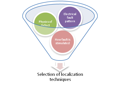
There are different techniques to identify failures localizations. Selection of the localization technique depends on the fault electrical signatures – given that a defect can lead to multiple electrical consequences, depending on how it is stimulated.
Il manque un tableau ICI
Evolution of Techniques/ performance & flexibility requirements
Addressing sensitivity & resolution requirement for 65nm/45nm/28nm , down to 16nm, time to results, new integration challenges ( SiP, Flip-Chip, etc…)
Sector Technologies offers best in class solutions for Electrical Failure Analysis and wide range of solutions for needs across FA (Failure Analysis) laboratory
Check how we address ALL needs for the most advanced nodes – check our Meridian family platform
- Enabling a comprehensive detection solution – Best in class backside
- Ensuring sensitivity even with low Vdd (i.e. lower signal to detect)
- Ensuring best localization of physical failure root cause, thanks to advanced resolution solutions
- Check how innovation can help you,
Enabling new fault coverage, like broken scan chain, thanks to the modulation techniques – check our LVx option
Enabling full wafer cover solution, enabling faster debug process for IDM (integrated device manufacturer) and foundries, enabling yield analysis – check our Waferscan solution
Extending efficient EFA toward new integrated package – check ELITE solution
