Nano Probing

Electrical characterization

Proven for 7 nm

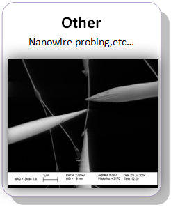
Solution for process characterization & failure analysis


NanoWorks® is the new product line from DCG systems, designed and optimized to electrically probe sub-100nm features on semiconductor devices.
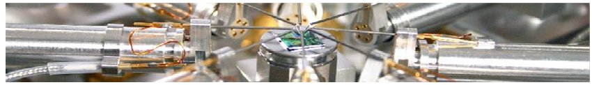
Nano Probing

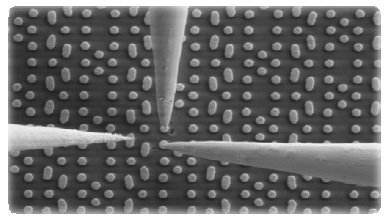
Nano Probing is a solution embedded or to be embedded into a SEM, based on state of the art nano probe, nano manipulation, motion control solution, flexible electrical characterization tool, together with other unique design/ tool to enable highest electrical probing quality (anti contamination system, etc…)

Nano Probing solution is being designed to provide the best Electrical probing quality together with an efficient solution package.

Electrical Probing quality – Stability & Repeatibility

  • Ensuring perfect probe positioning – thanks to direct SEM imaging
  • Anti – Contamination system solution
  • Under control SEM to ensure no impact for 7 nm

Efficient Probing – Landing & motion capabilities

  • Landing control –  open loop piezo creep control solutions & electrical feedback
  • Point & Click navigation
  • Enabling up to contact nano probing

Flexible configuration allowing multiple application

Flexible solution

A suite of nanoprobing characterization tools for the semiconductor industry and advanced research markets, including 8 probe systems

nProber IV HP: proven for 7 nm . 8 probes . High automation level .

nProber IV LR: proven for 7 nm . 8 probes . 

Hyperion II : proven for 7 nm . 8 Atomic Force probes . High automation level .

Applications

SEM nanoProbing enable multiple range of applications