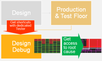
Supporting designer along standard silicon validation
Designer are used to debug through simulation, first from RTL level (Register Transfer Level), than functional and than at gate leval, however, the next level, debugging on silicon is more challenging: introducing new complexities & time delays.
Standard testing on silicon is using DFT & scan chains to support testability of their design. However production testing is mainly offering « go/no go » feedback. Practically, challenges for debugging on silicon are about :
Time to debug: When introducing silicon, manufacturing floor introduce delays – outsourcing test means design may start new project, while waiting being able to debug first one.
Complexity to debug: Designer are using EDA tools for Automatic Test Pattern Generation ( ATPG). Production test program translate pattern into their own language, introducing tool specificity. Complexity in translating back the test result for debugging.
Working around production Limitation: Test floor is focused in test application time, not debugging capabilities: limiting output to “go/no go”, thus debug capabilities
Speeding up silicon validation & easing interpretation for designer with decicate solution
Having a tester – specialized in debugging, accessible to designer/ product engineer. Than, Scan chains can also be naturally used to « debug » chip designs on silicon.
Teseda is offering this unique tester solution focused for design debug on silicon.
Accessible to designer/ product engineer, it speed-up access to the test capability
Using STIL language, it simplifies analysis, with design centric test result
Thanks to optimize memory, it enables efficient failure coverage, providing the required information for debugging