Solution for process characterization & failure analysis
Overview
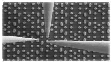
Nanoprobing is a solution embedded into the failure analysis workflow that is used for precise failure localization or characterizing individual transistors or devices down to single digit Nanometer technology nodes. There are two principles for probing: Secondary Electron beam Microscope (SEM) based systems and Atomic Force Microscopy (AFM) based systems. Each has its specific application range. Both system families are designed to deliver best in class electrical probing quality with an efficient solution package.
Core Technologies
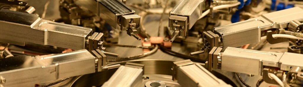
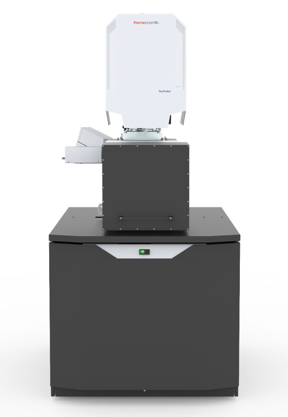
SEM based systems incorporate high precision probing mechanics and manipulators that are embedded in state-of-the-art SEM and operate under vacuum.
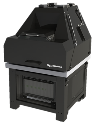
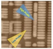
AFM based systems use AFM probes that raster the surface of the device for imaging and the same probes are used to electrically characterize it. The Hyperion II allows the operation in an N2 purged environment to minimize surface oxidation.
These systems are controlled through specific software packages allowing the user to precisely find the location or region of interest (ROI), land the probes precisely and acquire the required electrical response, i.e. I/V curves, C-V-curves, pulsed probing (possible for both tools set), EBAC/EBIC, EBIRCH for SEM based systems or pico current imaging and scanning capacitance microscopy (SCM) for AFM-based systems.
Solutions
A suite of
nanoprobing characterization tools for the semiconductor industry and advanced
research markets, including up to 8 probe systems.
nProber 4 LR
SEM based with imaging down to 150eV
Proven down to 5nm node
Cell counting function
8 probes
Guided operation
-40C up to 150C operation with thermal characterization package
SEM nanoProbing enable multiple range of applications.
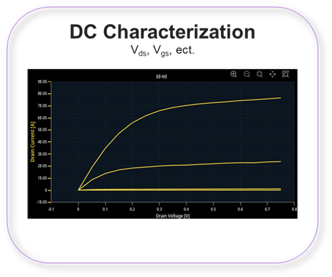
DC Characterization
Probing multiple transistors within the target area to localize a fault can be time-consuming. The NProber systems combine SEM imaging with I-V probing to quickly locate the area of interest and measure current-voltage curves.
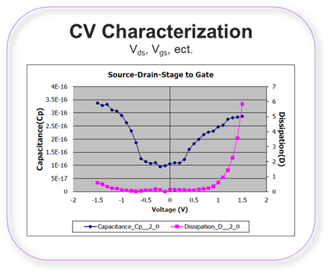
CV Characterization
C-V is used to study oxide layers, interface traps and charge carrier densities. The nProber systems offer high-resolution C-V with excellent impedance control, low leakage and very low noise.
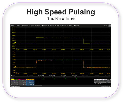
AC Characterization
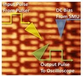
Pulsed I-V or AC measurements are used i.e. to determine signal rise-time delays of inverter stages.
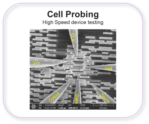
Cell Probing
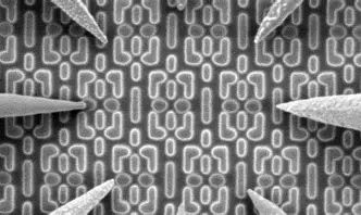
The nProber system is equipped with 8 high end manipulators each loaded with ultra sharp probe tips. With this setup the system allows to fully characterize the switching behavior of a 6T-bitcell (butterfly curves) or logic.
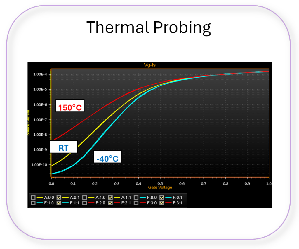
Temperature Characterization
The nProber system can be equipped with a thermal stage that allows device characterization in the temperature range from -40C up to +150C. This is needed for subtle and marginal fails.
This allows device characterization with AEC-Q100 (automotive) specs.
EBAC – EBIRCH
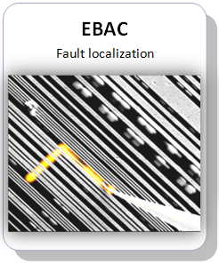
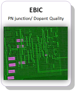
The nProber systems make use of the known SEMs based fault isolation methods EBAC (electron beam absorbed current) used to find i.e. metallization opens or shorts, EBIC (electron beam induced current) used to localize pn junction related failures as well as EBIRCH (electron beam induced resistance change) used to localize shorts in metallization and devices i.e. gate oxide failures in transistors.
The latest EBIRCH incorporates in total 12 different CC and CV amplifiers which allow investigation on even harder to localize defects.
Other
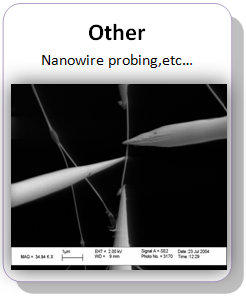
The nProber systems have a rather flexible configuration that would allow placing the probes also 3-dimensional structures such as nanowires.
AFM based applications
AFM nanoProbing enable multiple range of applications.
Current voltage (I-V) measurements
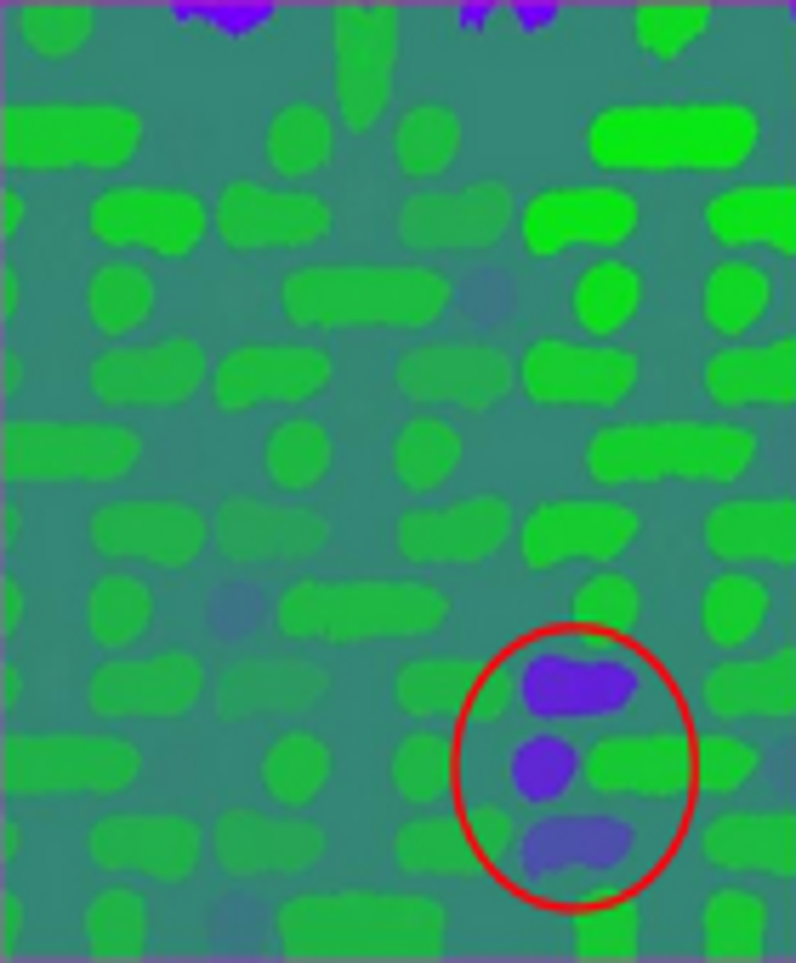
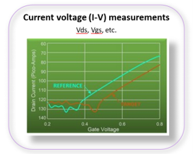
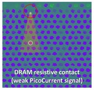
Probing multiple transistors within the target area to localize a fault can be time-consuming. The Hyperion II System combines PicoCurrent imaging with I-V probing to quickly find potential defects and measure current-voltage curves, without introducing measurement-related shifts.
PicoCurrent
PicoCurrent is a conductive AFM scanning technique that allows scanning and looking for non-analogous responses.
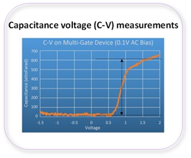
Capacitance voltage (C-V) measurements
C-V is used to study oxide layers, interface traps and charge carrier densities. The Hyperion II System offers high-resolution C-V with excellent impedance control, low leakage and very low noise.
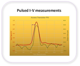
Pulsed I-V measurements
Pulsed I-V or AC measurements are used i.e. to determine signal rise-time delays of inverter stages or investigate resistive gate isolation failures as well as circuit level probing. As compared to the nProber systems the rise time characterization is a bit slower.