Advanced Optical Solutions for Semiconductor Applications
Overview
Seiwa Optical provides high-performance optical solutions for semiconductor failure analysis, inspection and imaging applications.
Its portfolio includes microscope objectives, infrared (IR) objectives, telecentric lenses, zoom lenses and advanced microscopy systems designed to deliver high resolution and sensitivity for demanding semiconductor applications.
High-performance optics are a critical component of semiconductor failure analysis and fault localization systems. Sector Technologies partners with Seiwa Optical to provide advanced optical solutions designed to improve imaging resolution, sensitivity and inspection capabilities.
A wide range of objective lenses and microscopy solutions is available to address different applications, wavelengths and system configurations, including frontside and backside semiconductor analysis.
Core Technologies
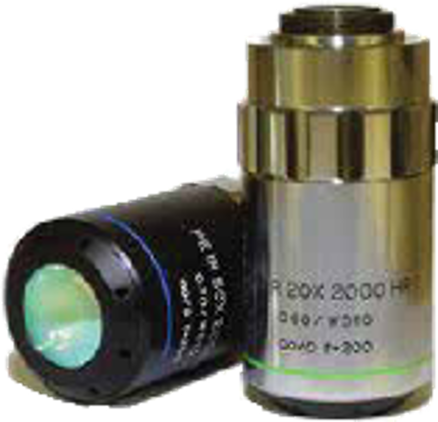
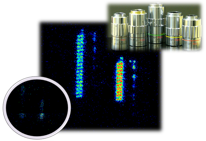
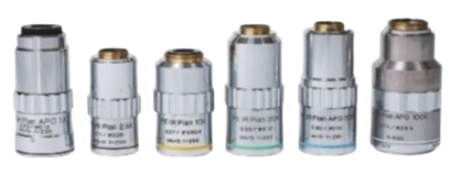
Optical & IR Objectives High-performance M Plan APO, PE IR and PE IR Hi-Res objectives for visible and infrared semiconductor imaging applications.
Telecentric & Zoom Lenses Precision optical solutions for inspection, measurement and imaging applications requiring high image quality and controlled magnification.
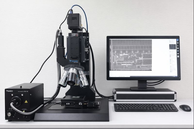
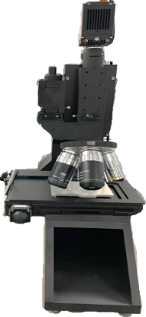
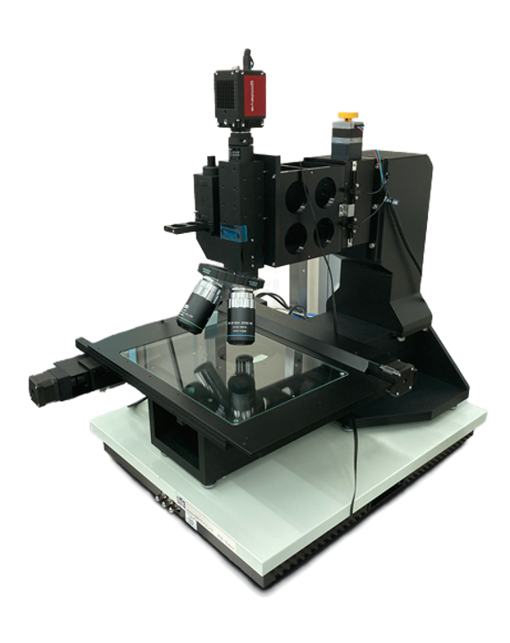
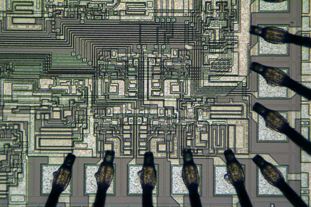
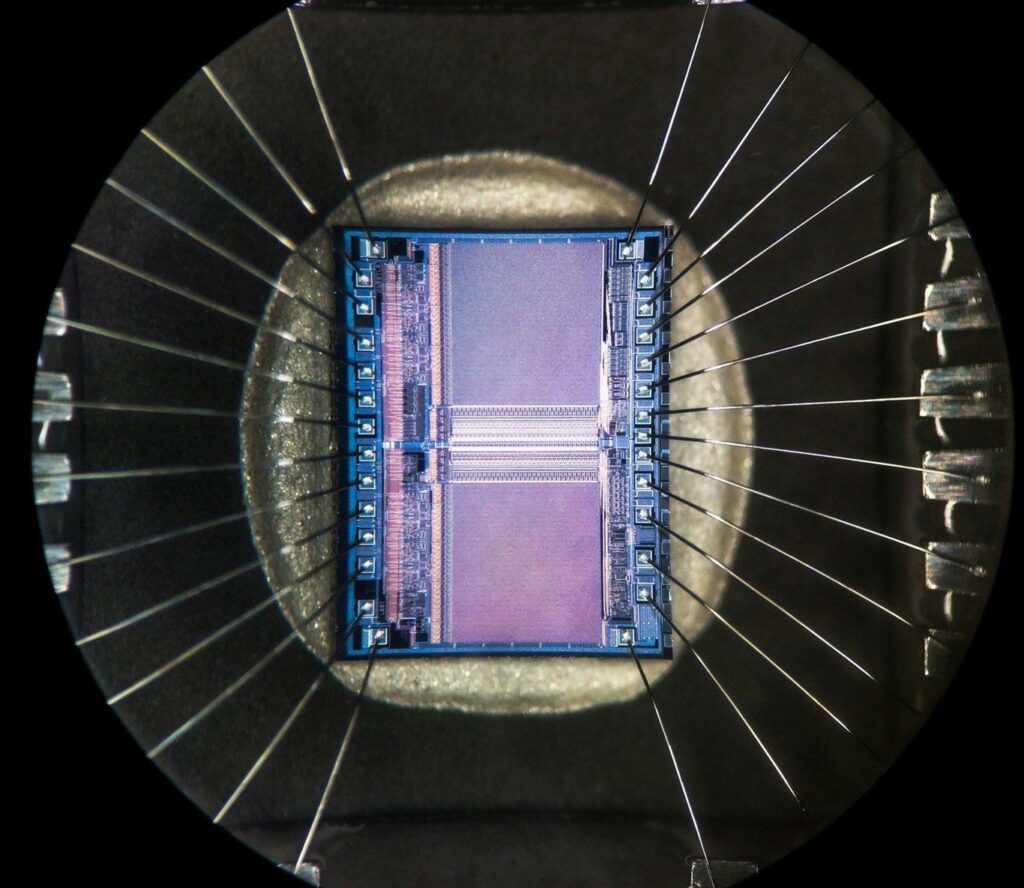
Microscopy Systems Advanced microscopy solutions for frontside and backside inspection of semiconductor devices, supporting the analysis of cracks, contamination, lamination defects, electrical discharge damage and other device anomalies.
Core Optical Solutions
Seiwa Optical offers a range of high-performance infrared objectives and microscopy solutions designed for semiconductor inspection, imaging and failure analysis applications.
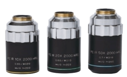
PE IR
Infrared Objectives for Semiconductor Imaging
High-performance IR objective lenses designed for backside semiconductor inspection and failure analysis applications.