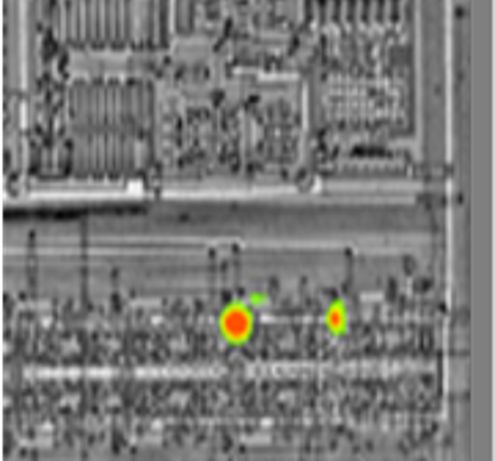
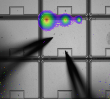
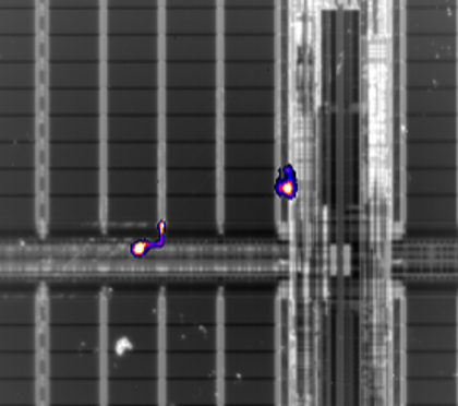
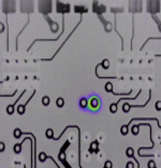
Static and Dynamic Failure Isolation for Advanced Semiconductor Devices
PCB, Package, Wafer and Die Analysis
Proven on technologies down to 7 nm
Overview
Rapid and accurate defect localization is essential for improving yield, accelerating product qualification, and ensuring the highest levels of product reliability. As semiconductor devices become increasingly complex, identifying electrical and physical failure mechanisms at microscopic scale has become a critical step in both development and manufacturing environments.
Sector Technologies provides advanced optical failure isolation solutions capable of localizing defects from PCB and package level down to individual transistors and interconnect structures. These technologies enable faster root cause analysis, reduced time to resolution, and improved manufacturing efficiency.
Core Technologies
Our portfolio combines the latest Thermo Fisher Scientific Electrical Failure Isolation (EFI) technologies, providing comprehensive solutions for defect localization across a wide range of applications.
From printed circuit boards and advanced packaging assemblies to full wafers and individual dies, our systems support failure analysis workflows throughout the entire semiconductor value chain.
Available technologies include:
Lock-In Thermography (LIT)
RF Lock-In Thermography (RF-LIT)
Optical Beam Induced Resistance Change (OBIRCH)
Photon Emission Microscopy (EMMI)
Laser Scanning Microscopy (LSM)
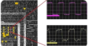
Laser Voltage Imaging (LVI)
Laser Voltage Probing (LVP)
Laser Assisted Device Alteration (LADA)
These solutions cover applications ranging from package-level fault localization to transistor-level defect identification.
Elite Family : Advanced Lock-in Thermography Solutions
The rapid adoption of 2.5D and 3D packaging technologies, increasingly complex interconnect architectures, and next-generation power devices has introduced significant challenges for failure analysis laboratories.
Defects often manifest themselves through localized power dissipation anomalies that generate subtle thermal signatures. Detecting and interpreting these signatures quickly is essential for accurate root cause identification.
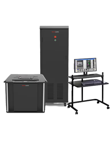
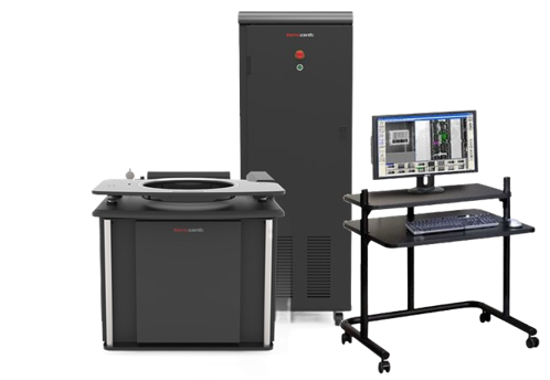
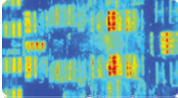
The Thermo Fisher ELITE platform provides highly sensitive, non-destructive fault localization through state-of-the-art infrared lock-in thermography. Patented noise-reduction technologies deliver exceptional thermal sensitivity, while integration with high-resolution laser scanning microscopy enhances defect localization accuracy.
For power electronics applications, the ELITE VX platform extends capability to devices operating at voltages up to 10 kV.
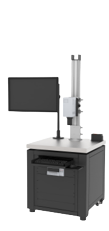
Elite Lite
Localization of shorts, leakage paths and open circuits in modules and packages
Meridian Family : Photon Emission and Laser Scanning Microscopy Solutions
The Thermo Fisher Meridian product family is designed for advanced photon emission microscopy and laser scanning microscopy analysis. The systems support static bias stimulation through probe cards or micro-probing platforms and deliver industry-leading sensitivity for electrical fault localization.
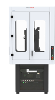
Meridian S
The Meridian S platform provides a cost-effective solution for routine failure analysis applications. It offers multiple photon emission detection options, dual-side probing capability, and a scalable upgrade path toward advanced dynamic fault isolation techniques.
Typical applications include:
Process monitoring
Design validation
Customer return analysis
Root cause investigation of random electrical failures
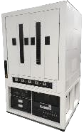
Meridian 4
The Meridian IV platform addresses the requirements of advanced semiconductor technologies where low-voltage operation, high circuit density, and complex failure mechanisms demand enhanced diagnostic capability.
Meridian WaferScan
Time-to-yield is a critical metric for both foundries and integrated device manufacturers. Waiting until dicing and packaging before identifying electrical defects significantly increases development costs.
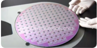
The Meridian WaferScan platform enables defect localization directly on production wafers using standard test infrastructure, including probe cards, load boards, and automatic test equipment.
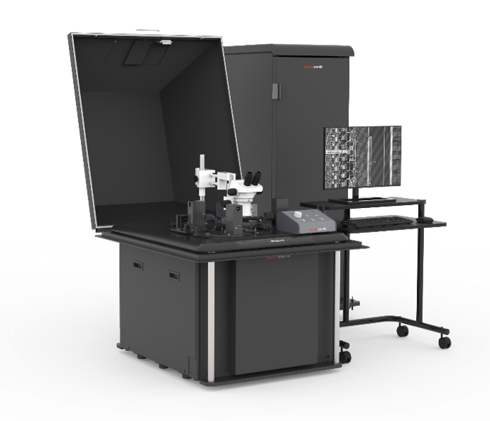
Meridian S
Key Capabilities
Localization of shorts, leakage paths and open circuits on silicon dies and wafer fragments
Static Photon Emission Microscopy
OBIRCH analysis
Solid Immersion Lens (SIL) technology
Available Options
High-voltage configuration for SiC and GaN devices