design or product engineer to quickly validate initial silicon, thereby saving weeks in the silicon verification process. It is focused to complete the scan chain debug, getting debug independent of outsourcing testing capabilities.
failure analysis engineer to support dynamics applications on their Electrical Failure Analysis applications – taking advantage of the portable, easy to use system to quickly diagnose issues as a stand alone system or in conjunction with leading FA equipment.
Core Technologies
Teseda is developping solutions to simplify approach for:
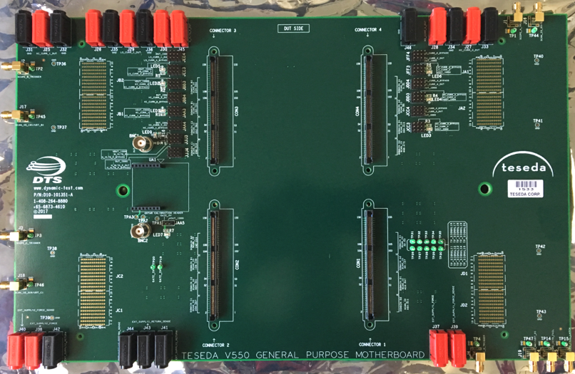
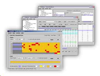
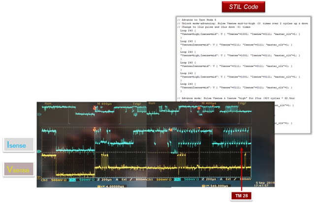
Developping Simple to Use Test solution – thanks to Teseda hardware plateform V550 , in conjunction with Teseda’s TWB. Input – Set-up – Analysis is simplified thanks to its unique structure: all results are still refering to your STILL structure.
Defect Isolation tool set – beyond Test results provided – Diagnostic ManagerTM(DM) software and Broken Chain Analyser (BCA) modules provide Defect isolation tool kit – the unique value is that it is simple to use and user keep control on its debug (unlike other EDA solution)
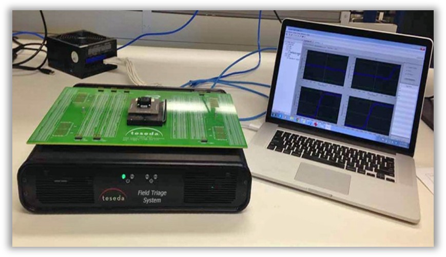
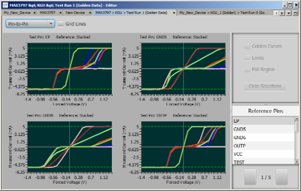
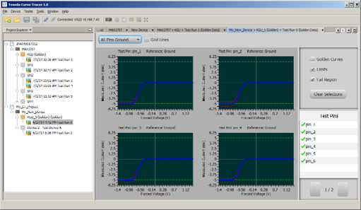
Field Triage package – Field Triage is a simple package, with « one button » solution to curve tracing, leakage & continuity testing – enabling fast response to your customer failure directly at your field offices. It is available either as a package with cut down version of the V550 or as a module of test solution above.
V550 Family Solutions
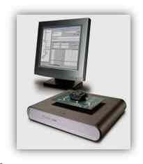
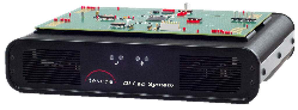
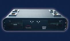
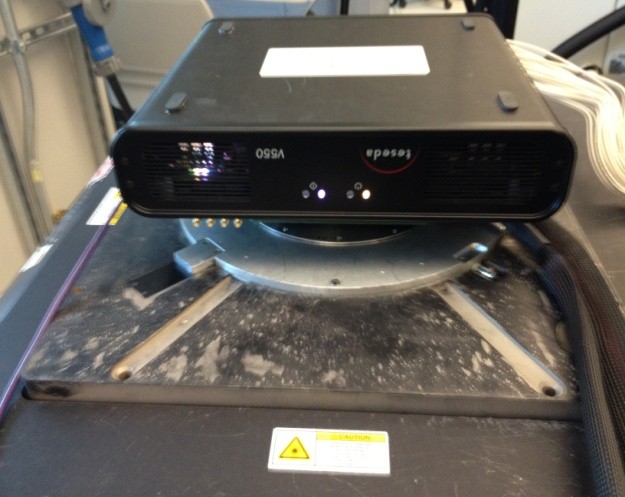
Teseda hardware plateform is an portable, easy to use tester system focused in enabling high failure coverage. Unlike production ATE, it has much more memory for failure capture. Its high failure coverage thus enabler designer scan chain debugging on silicon. It can be used as well of stimulus for the failure analysis equipements.
The V550 supports 512 pins configurable as either data or clock. It is available in an 80 MHZ scan rate version, and is upgradeable to 100 MHZ. The memory subsystem includes 32 Million Vector Drive/compare per channel (upgradeable to 64 Million), 40 Million Vector capture memory per channel and 16 Million Vector failure capture per channel.
The Teseda WorkBench™ (TWB) software exploits the full power of your DFT investment, enabling design, test, manufacturing and FA teams to work together to reduce time to production, accelerate yield learning, and maximize profits.
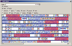
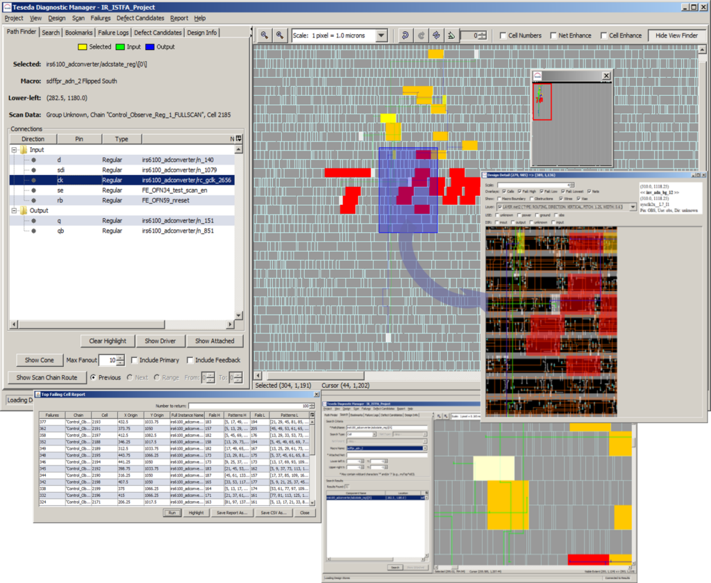
Diagnostic Manager (DM)™ quickly links structural test mismatch data to its physical domain for rapid analysis and diagnosis of defects and hot spots.
V550
512 I/O pins with up to 100 Mhz frequency
Supports functional and scan-based testing, BIST and IDDQ measurements
64Mb per pin pattern depth with up to 40Mb of acquire memory
Flexible, per-pin timing capabilities for complex testing needs
DC parametric and Curve Tracing options
Comprehensive fixturing and interfacing options
Portable, lightweight and air-cooled – weighs just 13.5 lbs
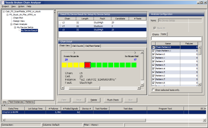
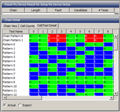
Teseda’s Broken Chain Analyzer fully exploits the power of your existing DFT-based tests to automatically analyze captured tester fail logs and detect all common causes of scan chain failures – both hard (stuck-at fails) and soft (timing or voltage-related fails) down to the failing bit location. The user simply executes a standard chain flush and a small sample of ATPG test patterns to capture a resulting fail signature. Fail logs can then be imported into Broken Chain Analyzer, along with the test pattern for automated failure diagnosis.
Diagnosis is performed using our interactive GUI, or diagnose multiple sets of captured fail logs via an automated batch mode. Diagnosed chain bit fails can then be easily analyzed by Teseda’s Diagnostic Manager NetXY™ to identify the physical location of the individual net that is the likely causing the failure in the scan chain.
Field Triage
Fast response time to your customer & Cut Factory Failure Analysis Loading by as Much as 40%.
Teseda’s DC Field Triage™ Package provides the user with easy to use, automated screening tools for DC related device failures. Designed for use by field personnel, the DC Field Triage Package puts device failure triage into the design and field support centers, enabling fast, timely and detailed responses to your customer’s quality concerns. Since first-level field screening is done in the field, factory failure analysis tasks are offloaded by as much as 40%.
Broken Scan Chain Analyser
Key Capabilities
Analyzes scan fail logs determine specific failing bit location within a defective scan chain
Works with all EDA-generated patterns and captured scan fail logs
Analyzes scan fail logs from any source
Identify the physical location of causes of scan chain faults
Locate and isolate the failing scan cell within a failing scan chain
Find broken scan chain
Link test fail to physical location
Device stimulation for failure analysis
Very easy setup inside OFI tools
No induced vibration
Interactive software for playing with parameters
Defect Isolation with DI software
Traverse through the physical design to trace nets and vias down to the defect location
Utilizes industry standard LEF/DEF design files, scan-based test information, tester fail logs and diagnostic reports to determine and isolate the physical defect location
Interactive layout viewer displays scan chains, mapped mismatches of scan cells, layers, nets and subnets with search capabilities (component, net, cell)
Physical XY coordinates are always displayed for components and nets to guide the user through the design to quickly identify suspect sites for FA using techniques like Emission, OBIRCH, LIVA, TIVA, or FIB
Compatibility with emulation and ATE-based workflows