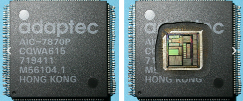
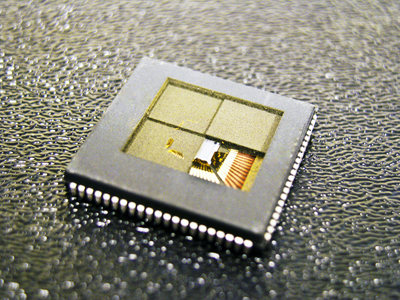
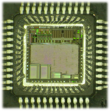
Sample preparation is a key step in Failure Analysis, enabling precise access to areas of interest while preserving device integrity.
It can be performed after a non-destructive fault localization, using the ELITE system, or during die inspection to target the regions to be analyzed.
Core Technologies
Package opening is performed using appropriate techniques (chemical, abrasive, or mechanical) to expose the silicon without damaging internal structures.
Silicon thinning (backside thinning) is done to continue with advanced analysis techniques, including LVx.
Custom sample preparation can be developed depending on the device architecture and the type of failure under investigation.
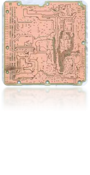
The preparation can also be carried out directly on PCB to isolate signals, facilitate measurements, reproduce specific operating conditions, or perform delayering.
All processes are executed faster, with precision, and in total control, ensuring reliable analysis results.
Decapsulation solutions
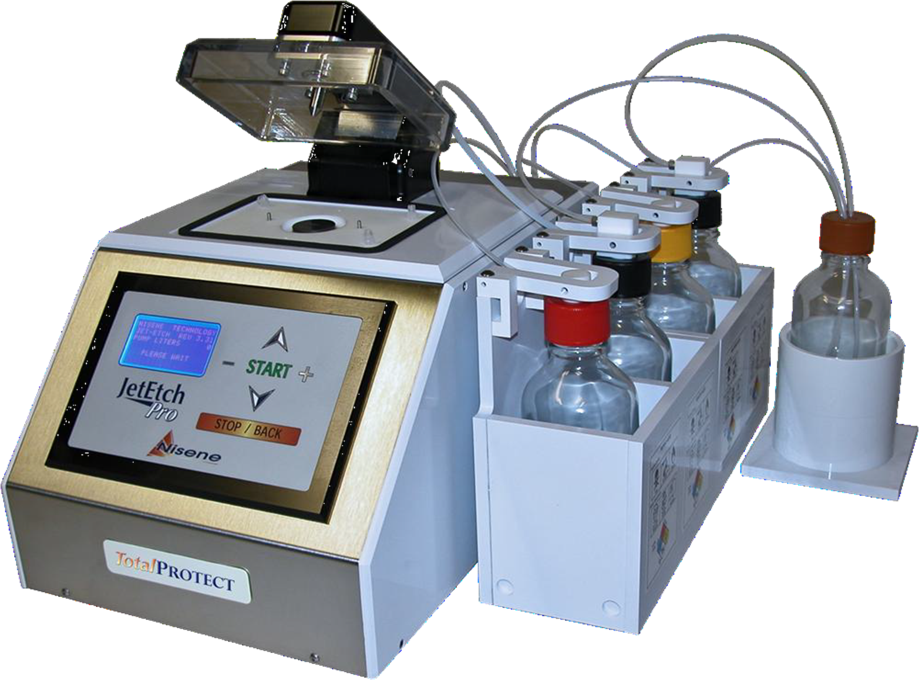
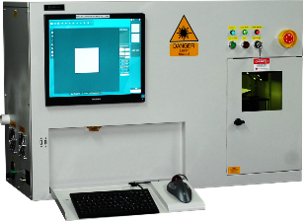
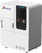
For over six decades, Nisene Technology Group has set the standard for precision, innovation and reliability in the semiconductor failure analysis and counterfeit detection industry. Advanced decapsulation tools, including chemical based JetEtch system, laser based pre-cavitation LE1064 and Microwave Induced PlasmaEtch IC decap solutions, empower engineers and researchers to perform critical IC (Integrated Circuit) analysis efficiently, cleanly, and safely.
We have raised the bar with the new line of automated Chemical IC Decapsulation systems, the JetEtch, CuProtect and TotalProtect. By offering three distinct IC decap systems with a single foundational platform Nisene can meet the specific needs of all customers seeking precision decapsulation for the types of ICs they are required to decap and perform the necessary failure analysis.
The latest PlasmaEtch, MIP 4761 is highly efficient in removing encapsulant while protecting the delicate bonding wires. The MIP 4761 proprietary etching process can safely and cleanly decapsulate your most difficult IC packages.
Laser decapsulation is a highly precise and effective method of removing plastic encapsulant material from a device. By using a 20W 1064nm laser, the encapsulant material is vaporized, eliminating the risk of accidentally destroying or washing away a defect with decapsulation chemicals.
JetEtch Pro family
JetEtch Pro — Standard chemical decapsulation CuProtect — Bias-assisted copper-wire protection TotalProtect — Bias control with sub-ambient etchant cooling
As new generations of IC’s and other microelectronics move to smaller and smaller node sizes, there is a need for novel QA/QC, V&V, and reverse engineering techniques that can resolve device structure at an incredibly small scale. Varioscale products aims to meet the needs of new device analysis with a novel suite of tools and methods that push the boundaries of imaging and sample deprocessing capabilities.
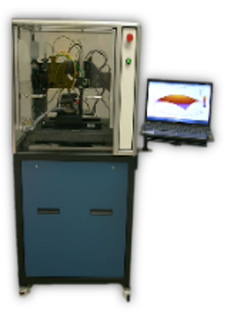
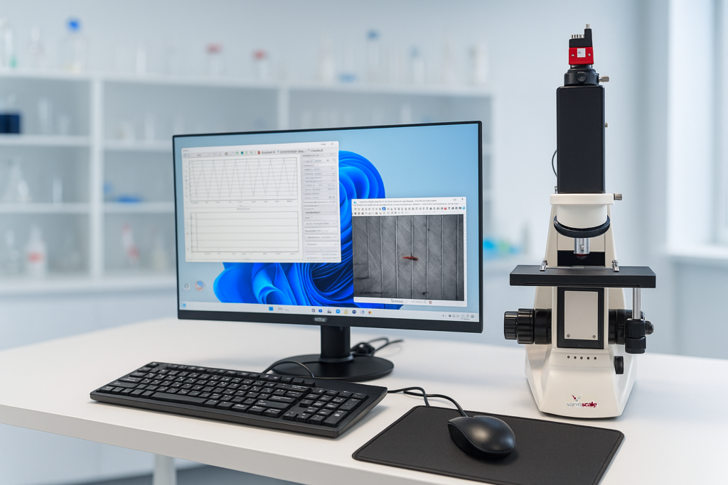
The VarioMill is uniquely suited for photoemission prep with its ability to automatically thin and measure parts down to less than 3 microns of remaining silicon thickness.
VarioMetric utilizes an interferometric measurement system to determine the thickness of a sample in real time. Using this technique allows rapid measurement and characterization of a part, necessary in the fast paced environment of the semiconductor industry. The VarioMetric system preforming this measurement and analysis is included in all Varioscale products: VarioEdit, VarioMill and VarioMetric. This metrology system combines the ability to determine a wide range of thicknesses and robustness of measurements even on rough and highly doped samples to create a uniquely useful measurement system. The dual spectrometer system employed by all state-of-the-art Varioscale products pushes the measurement capabilities to its current specification of 1000 um down to 500 nm in a single system.